
USB Switch Driving Unit
$1,000.00
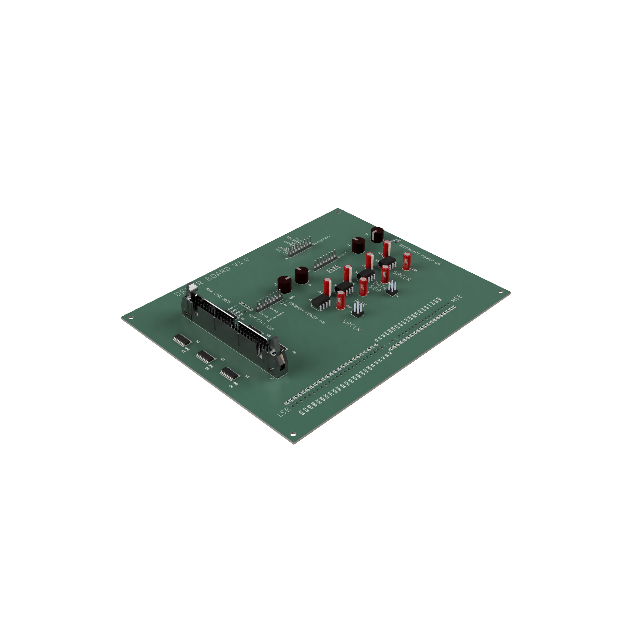
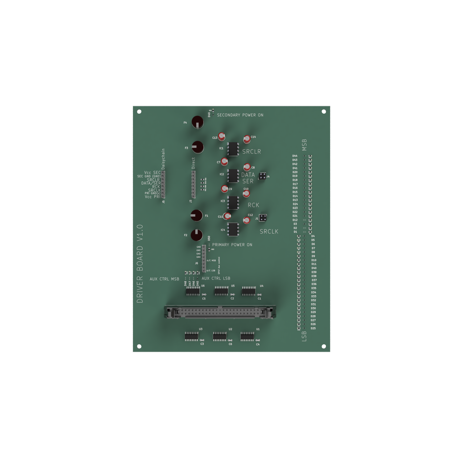
Our Switch Driver PCB is a high-capacity, USB-controlled logic driver designed to operate large networks of solid-state RF and microwave switches. Engineered for precision, scalability, and robustness, this board provides 44 logical outputs (48-bit addressing capability) to support complex switching architectures used in advanced test and measurement systems.

Our Switch Driver PCB is a high-capacity, USB-controlled logic driver designed to operate large networks of solid-state RF and microwave switches. Engineered for precision, scalability, and robustness, this board provides 44 logical outputs (48-bit addressing capability) to support complex switching architectures used in advanced test and measurement systems.
Purpose and Function
Modern RF switching networks—such as those used in multi-port VNA extension units—require reliable digital control with high channel counts. For example, our own 8-port VNA extension module incorporates 22 individual solid-state switches, each requiring 2 bits for full control. The Switch Driver PCB is built to meet and exceed these requirements.
With a single board supporting up to 48 bits of output, users can control large cascaded switch networks directly from a single USB connection. Multiple boards can also be tethered together, enabling the control of massive switching matrices with 128 channels or more, making the design ideal for scalable RF test systems, automated labs, and high-channel-count measurement platforms.
Scalable, USB-Based Control
Communication is handled via a straightforward USB interface, allowing the board to be controlled with simple software commands or integrated into automated test scripts. This flexibility makes it easy to manage:
Solid-state switch banks
Multi-layer RF routing structures
Programmable signal distribution networks
Complex multi-port VNA extension units
Robust Design for Harsh Electromagnetic Environments
To ensure reliable operation even in electromagnetically noisy environments, the board is built with optocouplers on the control lines. This design choice provides:
Electrical isolation between the host system and the switching network
Reduced susceptibility to EMI and ground noise
Protection of sensitive measurement equipment
Stable long-term operation in high-power or industrial RF settings
Key Features
USB-controlled 48-bit output for high-density switching
44 logical output pins for direct switch control
Modular architecture: multiple boards can be daisy-chained for >128 outputs
Ideal for controlling large solid-state RF switch networks
Optocoupler isolation for reliable performance in EMI-heavy environments
Compatible with programmable test setups and automation frameworks
Perfect companion hardware for multi-port VNA extension systems
Purpose and Function
Modern RF switching networks—such as those used in multi-port VNA extension units—require reliable digital control with high channel counts. For example, our own 8-port VNA extension module incorporates 22 individual solid-state switches, each requiring 2 bits for full control. The Switch Driver PCB is built to meet and exceed these requirements.
With a single board supporting up to 48 bits of output, users can control large cascaded switch networks directly from a single USB connection. Multiple boards can also be tethered together, enabling the control of massive switching matrices with 128 channels or more, making the design ideal for scalable RF test systems, automated labs, and high-channel-count measurement platforms.
Scalable, USB-Based Control
Communication is handled via a straightforward USB interface, allowing the board to be controlled with simple software commands or integrated into automated test scripts. This flexibility makes it easy to manage:
Solid-state switch banks
Multi-layer RF routing structures
Programmable signal distribution networks
Complex multi-port VNA extension units
Robust Design for Harsh Electromagnetic Environments
To ensure reliable operation even in electromagnetically noisy environments, the board is built with optocouplers on the control lines.
This design choice provides:
Electrical isolation between the host system and the switching network
Reduced susceptibility to EMI and ground noise
Protection of sensitive measurement equipment
Stable long-term operation in high-power or industrial RF settings
Key Features
USB-controlled 48-bit output for high-density switching
44 logical output pins for direct switch control
Modular architecture: multiple boards can be daisy-chained for >128 outputs
Ideal for controlling large solid-state RF switch networks
Optocoupler isolation for reliable performance in EMI-heavy environments
Compatible with programmable test setups and automation frameworks
Perfect companion hardware for multi-port VNA extension systems

Made in the USA
At Qubit Microwave, we strive for the highest quality products. All designs are fabricated in the USA, enabling streamlined production and competitive pricing without foreign tariffs.