
Microwave Switches for Quantum Computing
A conversation-friendly guide that still respects the physics—and helps you choose the right switch family for your system
Let’s start with the real problem you’re trying to solve
If you’re building or scaling a quantum computing platform, you’re not just building a qubit chip. You’re building a tightly-coupled microwave system where control pulses and readout signals have to arrive with the right amplitude, phase, timing, and noise floor—often while traveling through meters of coax, multiple temperature stages, and an environment where tiny imperfections turn into calibration drift or fidelity loss. That’s why the microwave systems perspective is now mainstream in the field: as qubit counts grow, the microwave “plumbing” and its stability become first-order constraints, not background details. 
Microwave switching becomes powerful in this moment because it’s one of the few tools that can reduce system complexity without changing your qubit physics. A switch can help you share expensive instrumentation, reduce the number of physical routes you must permanently wire, and make routing decisions in software instead of with a wrench and a warm-up cycle. The catch—and this is where serious teams pay attention—is that the switch must be “quantum-grade” in the only way that matters: it must be predictable, quiet, and stable in the environment where you place it.
What a microwave switch is doing in a quantum stack, step by step
Picture a typical microwave-based quantum system in slow motion. At room temperature, you synthesize tones and shaped pulses using sources, DAC/AWG channels, IQ mixers, and digitizers. Those signals run down into a cryostat where attenuation and filtering protect the qubits from thermal noise, and where readout signals returning from resonators are amplified (often beginning with a cryogenic low-noise stage) before they’re digitized at room temperature. When you insert a switch into this story, you’re inserting a controlled decision point: “Which route is active right now?” That sounds simple, but in quantum it can be the difference between a system that scales cleanly and one that becomes unmanageable.
You can place that decision point at room temperature for rapid automation and instrument sharing, or you can place it at cryogenic stages to reduce wiring fan-out and thermal load toward the coldest stage. This staged-architecture logic is not speculative; it shows up directly in published cryogenic control demonstrations. Hornibrook and colleagues, for example, demonstrate a micro-architecture that distributes classical control components across dilution refrigerator stages, including a cryogenic FPGA controlling a switching matrix at 20 mK that manipulates a semiconductor qubit.
Does switching “increase qubit count”?
It’s worth answering this plainly because it’s a common misconception. Switching does not increase the number of physical qubits fabricated on the processor. What it can increase is the number of qubits you can practically operate per cryostat and per rack—because it helps you reuse control and readout resources, reduce persistent wiring requirements, and make calibration and characterization workflows more scalable. In other words, switching increases addressability and operational throughput, not the lithographic qubit count.
This idea—classical I/O becoming the bottleneck—appears across quantum modalities. In trapped-ion quantum computing, for instance, the “wiring challenge” is treated as a serious scaling constraint, motivating architectures that integrate switching electronics (WISE) to reduce I/O requirements without compromising performance.
Multiplexing is where switches stop being “nice” and become “strategic”
Most teams become fluent in multiplexing in the same order their systems mature: first they time-share what they already own, then they frequency-share to read out more in parallel, and finally they combine approaches into hybrids that match their modular architecture.
Time-domain multiplexing (TDM) is the most intuitive starting point.
You route a high-quality chain to one destination at a time, then switch to the next destination on a schedule. TDM is naturally aligned with sequential workflows like device screening, resonance discovery, and recurring calibration sweeps. When you see demonstrations that bring switching into the cryostat control plane, what you’re really seeing is TDM being elevated from “rack convenience” to “scaling architecture,” because routing decisions closer to the qubits can reduce the number of permanent cold interconnects you need.
Frequency-domain multiplexing (FDM) attacks the problem differently.
It reads out multiple resonators (and therefore multiple qubits) simultaneously through a single line, separated by frequency. This is well established in superconducting readout. Jerger and colleagues demonstrate parallel readout of flux qubits using frequency-division multiplexing through one microwave line and discuss scaling implications. Heinsoo and colleagues later demonstrate rapid, high-fidelity multiplexed readout of five superconducting qubits within a single wide readout channel and report that simultaneous-readout errors remain close to individual-readout errors in their implementation—an important reality check on what good multiplexing engineering looks like in practice.
So where do switches fit if FDM already exists?
In the real world, FDM scales in banks. You build modules that can read out multiple qubits in parallel, and then the system needs to decide how many of those banks can share one high-performance amplification and digitization chain. Switching becomes the bank selector that lets you time-share expensive measurement chains across multiple modules while still using FDM inside each module. Once you think in banks and modules, switching becomes the mechanism that makes modular scaling economically and physically sane.
There’s also a more advanced frontier where switching is engineered specifically for cryogenic microwave multiplexing protocols. Chapman and colleagues describe and characterize a general-purpose cryogenic microwave device (a tunable inductor bridge-based element) that can rapidly switch modes and enable multiplexing protocols, including a two-channel code-domain multiplexing demonstration.  You don’t need this exact approach to benefit from switching, but it shows how seriously the field treats “programmable cryogenic switching” as a scaling primitive rather than a mere accessory.
Room Temperature
When the switch is at room temperature, it is usually easy to deploy, service, and validate. It can dramatically improve lab automation because you can reconfigure routing in software, share instruments across many devices, and reduce manual interventions. What it does not do is reduce the number of coax lines entering the cryostat or the thermal conduction those lines create. So room-temperature switching tends to be the fastest win for productivity, but not the deepest win for wiring scalability.
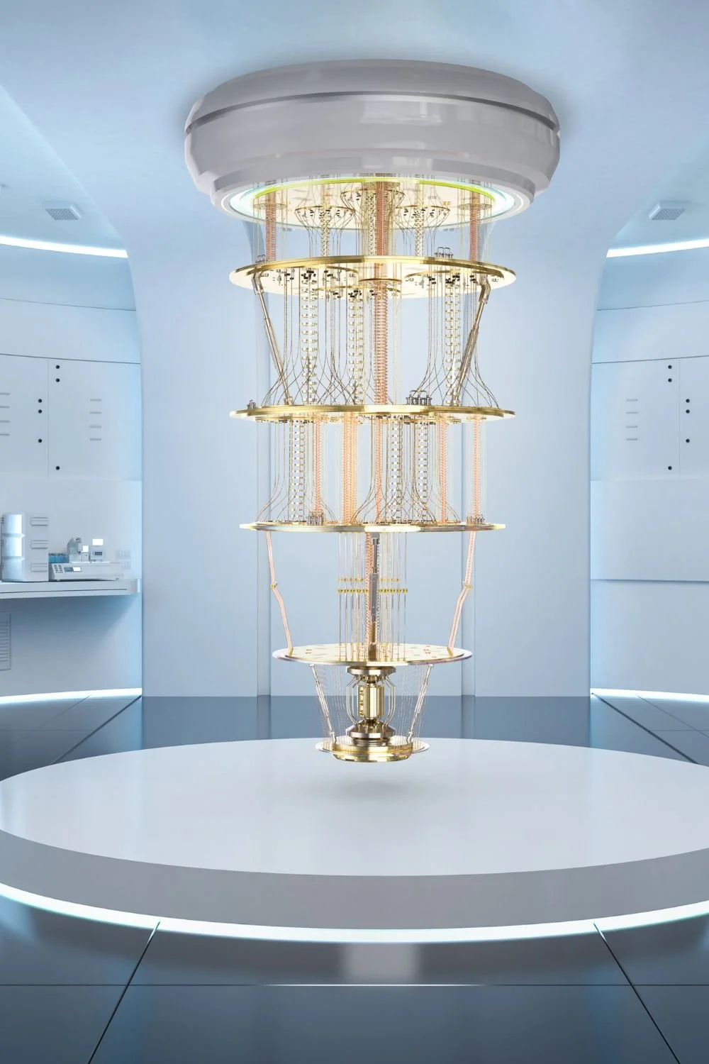
Where should the switch live: room temperature, 4 K, or millikelvin?
This is the most important decision you’ll make, because it determines whether switching is primarily a workflow tool or a wiring-scaling tool.
Cryogenic Stage
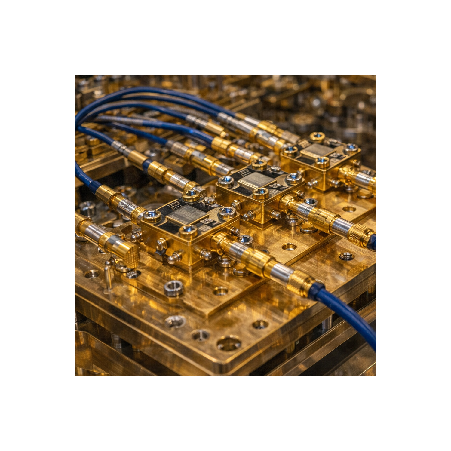
When the switch moves to cryogenic stages—often around 4 K—you begin to relieve the wiring burden toward the coldest stage because routing and fan-out decisions happen closer to the qubits. This is also where a lot of integration work is converging: the 4 K stage has more cooling power than millikelvin stages, but is close enough to reduce interconnect pressure meaningfully. Underwood and colleagues demonstrate cryogenic CMOS control electronics thermally anchored at 4 K that generate qubit control waveforms and enable a two-qubit cross-resonance gate, illustrating both the promise of moving classical functionality inward and the need to control leakage and spurious behavior.
Millikelvin Temperatures
When the switch lives at millikelvin temperatures, the wiring relief potential is maximal, but the constraints are brutal: dissipation budgets are tiny, control lines must be filtered to avoid injecting noise, and any spur or transient can become a fidelity problem. Still, the field is moving in this direction when it can be engineered responsibly. Bartee and colleagues demonstrate a heterogeneously integrated cryo-CMOS chip operating at millikelvin temperatures to control silicon spin qubits, explicitly motivated by the wiring density challenge and the need for dense chip-to-chip interconnects.
What “quantum-grade switching” really requires
If you’re buying a switch for quantum applications, the right mindset is to treat it as a part of your error budget and your calibration budget—not just a component with S-parameters. Insertion loss matters because any loss before your first low-noise amplification stage reduces the readout signal you can preserve and therefore degrades measurement margin. Isolation matters because leakage tones can become unintended drives or measurement backaction, especially in multiplexed systems. Matching and phase repeatability matter because quantum control depends on phase-coherent pulses and stable transfer functions; if routing changes phase unpredictably, your calibrations become fragile and expensive to maintain. 
The “quietness” of switching is equally important and often underestimated. In quantum systems, you care not only about the RF path but also about what the act of switching injects into the environment: transients, spurs, EMI from control lines, and route-dependent settling behavior. This is why credible quantum switching discussions increasingly emphasize temperature-relevant validation rather than relying solely on room-temperature datasheets. A good example of that style is cryogenic evaluation work on commercial SP4T MEMS switching aimed at cryogenic multiplexer viability, where the device is characterized at cryogenic temperatures specifically to assess suitability for quantum interconnect architectures.
The product families, explained like you’re choosing tools—not memorizing parts
What architectures are used today, and how switching improves them
Most deployed quantum microwave architectures today still resemble a “many cables, many instruments” model: multiple room-temperature channels feed multiple cryostat lines, and readout is increasingly multiplexed but still constrained by amplifier chains and digitizer resources. That model works well for small-to-moderate systems, but it becomes painful as channel counts rise because wiring, calibration, and maintainability scale poorly. The microwave systems review emphasizes that these microwave-engineering concerns become the practical bottleneck for scaling, which is why switching and integration are now treated as architectural levers rather than accessory choices. 
Switching improves today’s architectures in a very specific way: it lets you separate “how many endpoints exist” from “how many high-performance chains you permanently dedicate.” In near-term systems, that means using room-temperature matrices to accelerate characterization and using switching between readout banks to share expensive measurement chains. In mid-term systems, it means pushing bank selection and routing into cryogenic stages to reduce the number of cold interconnects required. In longer-term systems, it means integrating routing and control into cryogenic electronics so that the wiring challenge is addressed structurally rather than incrementally. The same motivation—reducing I/O while preserving performance—shows up in architectures like WISE for trapped ions and in cryogenic control electronics demonstrations at 4 K and millikelvin.
How to think like an expert buyer without turning it into a PhD thesis
An expert buyer starts by placing the switch in the architecture, because that tells you what matters. If the switch sits upstream of the first low-noise gain stage in a readout chain, insertion loss is sacred and cryogenic characterization is non-negotiable. If the switch is used for active multiplexing, repeatability, transients, and settling become as important as “static” S-parameters. If the switch is used in an FDM-heavy environment, linearity and isolation under multi-tone excitation matter because unwanted products can land in-band. And if the switch is going into the cryostat, power dissipation, thermal-cycle stability, and control-line hygiene become part of the RF spec whether the datasheet admits it or not.
That’s also the most honest way to sell quantum switching: you don’t promise miracles. You show that you understand where the switch sits, you provide the temperature-relevant data, you show repeatability and stability, and you help the customer map your component into their SNR and calibration budgets using the same system-level logic the literature is already using.
-
(These are the core sources underpinning the architectural and experimental claims above.)
1. J. C. Bardin, D. H. Slichter, D. J. Reilly, “Microwaves in Quantum Computing,” IEEE Journal of Microwaves 1(1), 403–427 (2021), DOI: 10.1109/JMW.2020.3034071. 
2. J. M. Hornibrook et al., “Cryogenic Control Architecture for Large-Scale Quantum Computing,” Phys. Rev. Applied 3, 024010 (2015), DOI: 10.1103/PhysRevApplied.3.024010 (includes cryogenic FPGA controlling a switching matrix at 20 mK). 
3. M. Jerger et al., “Frequency-division multiplexing readout and simultaneous manipulation of an array of flux qubits,” Applied Physics Letters 101, 042604 (2012), DOI: 10.1063/1.4739454. 
4. J. Heinsoo et al., “Rapid high-fidelity multiplexed readout of superconducting qubits,” Phys. Rev. Applied 10, 034040 (2018), DOI: 10.1103/PhysRevApplied.10.034040. 
5. B. J. Chapman et al., “General purpose multiplexing device for cryogenic microwave systems,” Applied Physics Letters 108, 222602 (2016), DOI: 10.1063/1.4952772 (demonstrates rapid switching enabling multiplexing protocols, including code-domain). 
6. M. Malinowski, D. T. C. Allcock, C. J. Ballance, “How to wire a 1000-qubit trapped-ion quantum computer,” PRX Quantum 4, 040313 (2023), DOI: 10.1103/PRXQuantum.4.040313 (WISE architecture integrating switching electronics to reduce I/O). 
7. D. L. Underwood et al., “Using Cryogenic CMOS Control Electronics to Enable a Two-Qubit Cross-Resonance Gate,” PRX Quantum 5, 010326 (2024), DOI: 10.1103/PRXQuantum.5.010326 (4 K cryo-CMOS control; discusses leakage/spurious considerations). 
8. S. K. Bartee et al., “Spin-qubit control with a milli-kelvin CMOS chip,” Nature (2025), DOI: 10.1038/s41586-025-09157-x (mK cryo-CMOS motivated by wiring density challenges).